Analog CMOS Integrated Circuits
Last semester given: 2021-22 Fall
Textbook: Behzad Razavi, “Design of Analog CMOS integrated circuits”, McGraw Hill (2000)
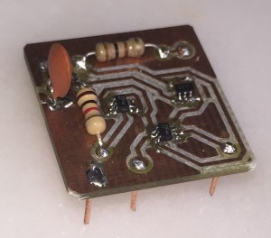
In the Spring of 2015, the first project assigned to students was to design and build an OPAMP using discrete nMOS and pMOS surface-mount transistor pairs. The students designed the OPAMP and built it on a 2cm x 2cm printed circuit board. Then, they measured the DC and AC electrical characteristics of the OPAMP to compare with the LTSpice simulations. The project was done in three phases: Simulation, PCB design, and measurement. The specifications included current consumption, output swing, input-common-mode range, open-loop gain, phase margin, slew rate, step-response, and small-signal gain-bandwidth product. The image below shows the OPAMP designed and fabricated by Burak Tekcan, consisting of three pairs of MOS transistors.
The second project assigned was the design of a temperature-independent voltage-reference circuit using a 0.7μm analog CMOS process. The stability must hold in the temperature range -20ºC to +80ºC. Students used CAD tools to simulate and generate the layout of the circuit.
Subjects covered:
- Single-stage amplifiers Chap 3
- Differential amplifiers Chap 4
- Current mirrors Chapter 5
- Frequency response of amplifiers, Miller effect Chap 6
- Operational amplifiers Chap 9
- Slew rate, Power supply rejection Sec 9.8
- Stability and frequency compensation Chap 10
- Review of MOS Device Physics Chapter 2
- Noise in amplifiers Chap 7
- Feedback Chap 8
- Bandgap references Chapter 11
- Switched capacitor circuits Chap 12
- Nonlinearities, linearization Chap 1 3
- Offset Chap 13
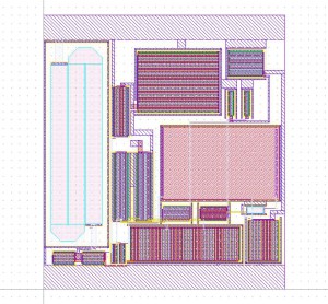
The image below shows the layout of a transimpedance amplifier including its feedback resistor.