
Introduction to CMOS VLSI Design
Last semester given: 2019-20 Fall
Textbook: Weste and Harris “Integrated Circuit Design (4th Edition)”(2010)
Software tool: Cadence v.6.1 running on CentOS Linux with Europractice license.
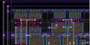
In the Fall of 2015, the students designed a 64-input OR/NOR gate using a cell library, starting from schematic entry and simulation for the purpose of obtaining a fast gate. They generated a layout of their gate and performed a post-layout simulation. The image below shows one corner of the design of one of the students.
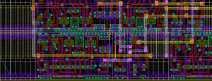
As their second project, using the same cell library, the students designed an 8-bit adder to be as fast as possible. They simulated the adder after schematic entry and performed a post-layout simulation after the layout. First, they used the conventional method: Schematic entry and layout. They also learned how to generate the design using the RTL compiler automatically. The image below shows a small portion of a typical layout.
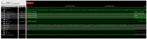
In the Fall of 2019, the students designed a 64-bit programmable digital correlator. They first developed a VHDL description of the correlator and tested its functionality using the Incisive tool of Cadence. The figure below shows the timing of the design for one of the students.
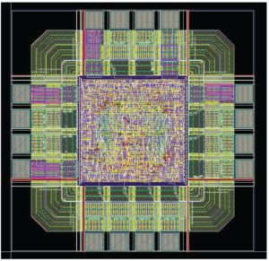
Then, the students synthesized a gate-level Verilog description using the Genus tool of Cadence. They performed a placement and routing using the Innovus tool of Cadence. They resynthesized the logic to include scan flip-flops for testability. They used the Modus tool of Cadence to generate test patterns to test the chip after fabrication. They also used the Tempus and Voltus tools of Cadence to perform accurate timing and power simulations. The final result was a GDS2 file of the chip, including the bonding pads, ready to be sent for fabrication. The picture below shows one of the layouts generated by one student.
Subjects covered:
- CMOS Logic, Fabrication and Layout
- CMOS Device Physics and Models
- DC and transient response
- Delay models
- Logical effort
- Dynamic and static power
- Interconnects
- Combinational circuits
- Sequential circuits
- Adders
- Comparators, counters, and others
- Multipliers
- Memories,
- Design for testability